National Geographic for Disney/Adam Geiger


Educational Innovations and Science Direct
Recommended
Recommended
Members Only Content


SEARCH FOR DATA SHEETS, PRICE, STOCK, AND PART STATUS OF ELECTRONIC COMPONENTS
SEARCH FOR DATA SHEETS, PRICE, STOCK, AND PART STATUS OF ELECTRONIC COMPONENTS
Learning Resources
Learning Resources


Sponsored Content
Sponsored Content
Industry Insights
Industry Insights

19425571 © Jakub Jirsak | Dreamstime.com

311250589 © Anatolii Savitskii | Dreamstime.com
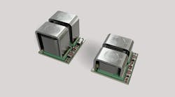
Keysight and Dreamstime_lescunliffe_23231826
Dreamstime_warutsintapanon_111244594
Dreamstime_generated_by_ai_maxkabakov

Dreamstime_pojoslaw_305383108


Dreamstime_kiosk88generated_by_ai_11195757


Dreamstime_ronstik_111023808


Dreamstime_alekseigorodenkov_30
Dreamstime_suwinpuengsamrong_139968432
114496245 © Kawee Wateesatogkij | Dreamstime.com
260215519 © Scharfsinn86 | Dreamstime.com

Embedded World


1025574 © Dana Rothstein | Dreamstime.com
Stanford University and Amazon
Dreamstime_luisfilipemoreira_309156038

Tero Vesalainen | Dreamstime.com


Dreamstime_ekkalucksangkla_1082822391

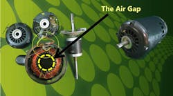
Best Electric Machine/YouTube
Dreamstime_atmosphere1_145936514
Dreamstime_artinun_prekmoung_146913868
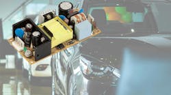

Cabe Atwell/Electronic Design
Muhammad Shoaib, Dreamstime
309588159 © Alexei Onufriiciuc | Dreamstime.com

Andrei Dzemidzenka, Dreamstime


Electronic Design
Dreamstime_luchschen_26003212
Dreamstime_forfunlife_17805192
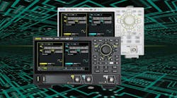
RIGOL Technologies